Central Air Data Computer
|
Note from the editor: This page is part of a collection of articles on the Thocp site because of its historic importance. This paper by Ray Holt reflects the creation of the first CPU chip
set. |
|
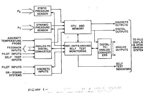
This paper describes the architecture of the CPU and Memory for the Central Air Data Computer (CADC) System used in the Grumman/ Navy F14A carrier-based fighter aircraft. The CADC performs specialized computational functions in response to input stimuli such as pressure sensors, temperature sensors and closed loop feedback inputs. Outputs from the CADC system are used to drive pilot visual displays (such as, altimeter, temperature indicator, mach number indicator, etc.) and to provide control inputs for other aircraft systems. The outputs from the CADC are in the form of digital and analog signals. Figure 1 illustrates a block diagram for the CADC. Being in a flight environment meant that certain constraints must greatly reflect the architecture of the CPU and Memory. These constraints were six, power, real-time computing capability and cost, not necessarily in that order. Other constraints such as temperature, acceleration and mechanical shock affected the overall design of the CADC. The size of the CPU-Memory was limited to a maximum of 40 square inches. This included the arithmetic section, read-only memory, and read/write memory. Since the unit was to be packaged on a printed circuit card the number of layers of the p.c. card was an important consideration. The power consumption had a limit of 10 watts at ambient 250C. This was principally a function of the capabilities of the p.c. card to withstand the heat. The required computing capacity for the CPU was not defined at the beginning. This meant that the system had to be somewhat flexible to changes in computational load. Of course limits had to be set to be able to work within the other constraints. What was known about the computation was the form of the equations to be implemented. This included polynominal evaluations, data limiting, data comparison and discrete or flag inputs and outputs. This meant that the arithmetic and logical functions of the system had to handle at least the following operations:
The last constraint of cost was certainly important since the system would eventually go into high volume production.
FUNCTIONS TO BE IMPLEMENTED Before we proceed, a better understanding of the functions to be implemented is necessary. The function that most often occurred was the polynomial, F(x) = a6x6 + a5x5 + a4x4 + a3x3 + a2x2 + a1x1 + a0 where x was the input, either from outside the CPU (sensors) or from its own memory. In order to save arithmetic. Time the polynomial was implemented in its "nested" form as follows:
F(x) = ((((((xa6) + a5 ) x + a4 ) x + a3) x + a2) x + a1) x + a0
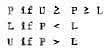
The data limit function was one that would accept 3 binary inputs, an upper limit (U), a lower limit (L) and a parameter (P). The output would then be as follows;
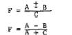
Even though such a function could be programmed in software, it was decided to build it in hardware since it was used often enough. Data conditioning and scaling also had to be accomplished. This involved the following simple expressions:
Again the occurrence of these were frequent enough to warrant hardware consideration. This will become apparent later when the hardware is discussed. Since size and power consumption was of the ultimate importance, MO S technology was chosen as the means of circuit implementation. This allowed greater packaging densities to he obtained that otherwise would not be. The slowness of MOS devices and the high thresholds used allowed a design that was virtually immune to electrical noise on the ground or transmitted from packages within close proximity. The higher supply voltages required resulted in a more efficient power supply design.
NUMBER SYSTEM The CPU is a fractional fixed point machine with the most significant bit a sign bit and the other bits representing data. Negative numbers are represented in two's complement notation. Two's complementation was chosen to avoid the ambiguity of double zeros. The word length chosen for the system was 2C bits; 19 bits of data and 1 hit for sign. This length was chosen after a thorough analysis of the accuracy required for certain throughput calculation! such as the rate of change of altitude function. Early in the architecture study it was realized that package size and quantity should be kept to a minimum if we were to meet the size constraints established. With minimum packaging space requirements it was necessary to use packages with the fewest possible leads. This would minimize the complex p.c. card interconnect which was inevitable. Because of this the processor was designed to transfer data serially throughout the entire system.
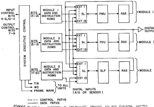
PROCESSOR PARALLELISM As is known by all computer designers, serial machines are usually not the best way to go if computational speed is needed. To get around this it was decided to have several arithmetic or processing units working at the same time. This resulted in a technique known a "pipeline processing" or "pipeline concurrency". As defined by Bell and Newell(2) "pipeline concurrency is the name given to a system of multiple functional units, each of which is responsible for partial interpretational and execution of the instruction stream." This system uses multiple functional units each dedicated for a specific task. These functional units are. 1. Parallel Multiplier
Unit (PMU) Figure 2 shows a block diagram of the functional units as they would work together in a typical system. Each unit was designed to operate as separate entity and could be used without the need of any of the other units. This was done to provide maximum expandability with minimum additional hardware. Each functional unit is controlled by its own micro-instruction ROM. The microinstructions are also transferred serially to minimize package pin count, Temporary data storage is provided in the form of read/write memory.
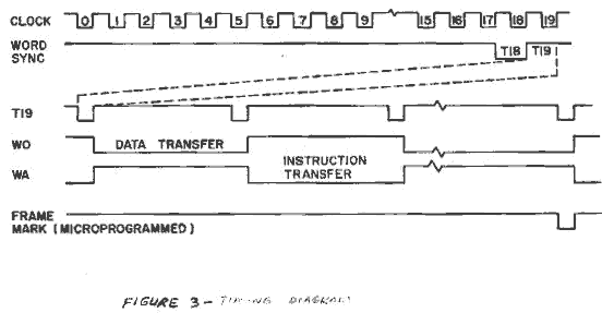
Before looking at the functions of each of these units a brief look at the timing is needed. Figure 3 illustrates this timing. The CPU-Memory clock is 375KHz. One complete clock period, defined as a bit time is 2.66usec. Every 20 consecutive bit times are defined as a word. The first bit time of a word is called TO, and the last time of the word is called T19. Two types of words are used in the system, WA and WO in WA, the arithmetical algorithms operate and instruction words are shifted serially into each functional unit. In WO, computational inputs and outputs are shifted serially among the units. A word mark used to distinguish word times is a signal coincident with T18 of every word time. Two consecutive word times, WA and WO, is called an operation (op) time. To distinguish the final operation time a frame mark is generated in the system executive control. The time between frame marks is called a frame. A frame includes one complete cycle of computations. The frame mark is microprogrammed to allow the user to restart the computational cycle when all previous computations are complete. Since this system must operate in real time it was therefore necessary to obtain the most computation from each functional unit during each frame time.
ARITHMETIC UNITS The Parallel Multiplier Unit accepts two serial inputs, multiplicand and multiplier, in one word time (WO) and produces their properly rounded product by means of a parallel algorithm in one more word time. The product is shifted out in the next WO, while inputs for the next operation are simultaneously shifted in. The multiplication operation is achieved using Booth's algorithm 2. The PMU does not used an instruction word to operate, but is capable of operating continuously in this manner. The Parallel Divider Unit accepts two serial inputs, dividend and divisor, in one word time (WO) and produces the proper quotient(3)
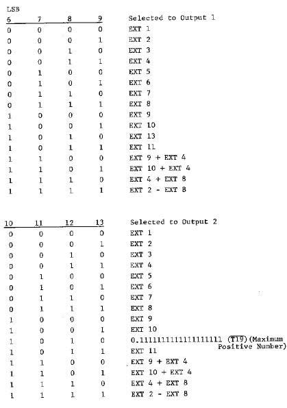
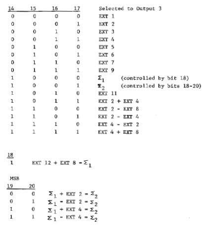
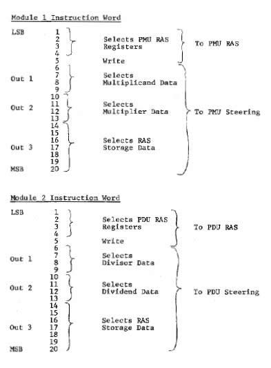
by means of a parallel algorithm in one more word time (WA). The quotient is shifted out in the next WD, while inputs for the next operation are simultaneously shifted in. The division operation is achieved by using a non-restoring division algorithm 3. An actual photograph of the PDU chip is shown in Figure 4. >The Special Logic Function performs logical operations and generates specific data and logic outputs. The unit accepts an instruction ward which specifies details of the operation. The fundamental logical operation of this unit is the limit function. It consists of three registers (U,P, and L) whose inputs arrive in WD. One of these registers is picked at the end of W0 >by associated comparison logic. Other logic functions such as AND's, OR's, GRAY CODE (special), Conditional, and Unconditional data branching is also included in this logic. The Data Steering Unit operates as a three channel serial digital data multiplexer. Information is shifted serially through the device during WD. A 15 bit instruction word is accepted during WA that specifies which input or input combinations (Add or subtract) is to be "steered" to each of three data outputs. The instruction word for this unit is the last 15 bits of the 20-bit instruction word. From the least significant end, the first four bits specifies the selection for Output 1. The next four bits specifies the selection for Output 2 and the last >seven bits specifies the selection for Output 3. Addition or subtraction is performed by specifying that output combination to be "steered" to the output. By performing additions and subtractions in this manner the programmer can obtain the sum and difference during the same word time that the data is being transferred. This transfer may be either to or from the memory or arithmetic units. Specific instruction codes are interpreted as follows: (4)
Since each SL has three outputs the capability is there to perform three additions and/or subtractions during one word time. Output 3 has the added feature of performing two additions during the same data transfer. This would be A + B + C. This feature was incorporated to handle the many cases of concluding a polynomial evaluation and adding another value to it. This would look like (Alx+AO) + Y.As the product of Alx is being transferred to memory the AO constant and Y value can be added to it. As can be seen the addition and subtraction, if used properly, can take 'zero' time since transferring of data has to be accomplished anyway. These four units comprise the hardware that can perform arithmetic operations. As shown in figure 2 each PMU, PDU and SLF has a Data Steering Unit associated with them. As will be discussed later this allows many data paths to be operating consecutively. Thus computational power is greatly increased.
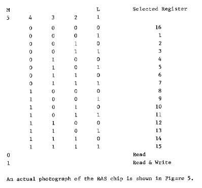
MEMORY UNITS There are two memory units, Read-Only Memory (ROM) for instruction storage and Random Access (Read/Write) Storage (RAS) for intermediate data storage. The ROM operates as a 2560-bit random access/sequential access device. It internally stores fixed patterns of 128 words of 20 bit length for serial readout. The patterns are specified by the user. The ROM has provision to accept a 20-bit serial binary word address. The first seven bits indicates which of the 128 words is to be accessed, and the next three bits specifies, by manufacture mask decoding, which ROM out of a possible eight ROM group should have its output enabled. The address management is accomplished by a register counter contained within the ROM. This counter has the following capability:(1) resettable, (2) steppable such that the memory can be sequenced through the 128-word field, (3) accepts a retain address command and holds the present address, and (4) accepts a numerical input for independent address modifying or loading. To accomplish the above address management, six logic inputs (reset (R), retain, increment, load, add, sub) and one address data input are provided. The address field is defined as follows: the first seven LSB's will select one of 128 20-bit words. The next three will be used to select one of eight ROM's, the remaining ten will be zero. The three-bit select field will determine, by mask deceding, which chip's (ROM) output is to be enabled. ROM's that are not enabled by the chip select field have disabled their outputs. The particular application described in this paper uses the ROM in the sequential access mode only. The RAS memory operates as s 16-word random access readwrite storage device. Information is shifted serially into and out of selected registers during WO. Memory readout is nondestructive, i.e., if a register is selected to be read only, then the data are also rewritten into the selected register. The RAS accepts an instruction word of 5 bits during WA. The least significant four bits o£ the instruction word specifies one of sixteen 20-bit serial registers. The contents of the selected register is shifted out to the data output serially during the next WO and WA. At the WO time, information from the data input is written into the selected register if the fifth control bit is a "1". If the fifth bit in a "0", the register contents remain unaffected. An external logic input "inhibit write" is provided to inhibit writing. The instruction word selects registers according to the following configuration:
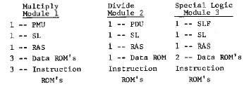
SYSTEM OPERATION AND INSTRUCTION FORMAT This processor uses a total
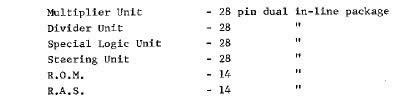
of 28 circuits. 1 -- Parallel Multiplier
Unit (PMU) The modules are as follows:
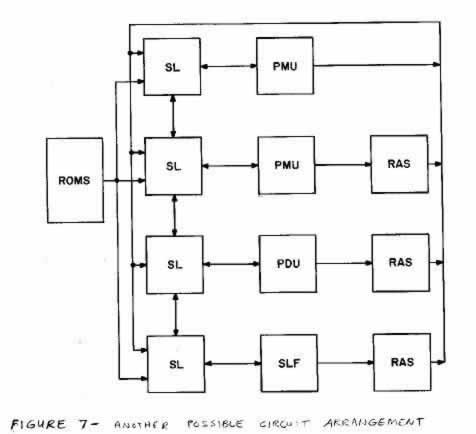
Each arithmetic unit has an associated steering unit and RAS unit. This is not an absolutely necessary association but is chosen to add flexibility to the programming. Figure 7 illustrates another possibility of a circuit arrangement. It is important to note that the hardware arrangement is flexible to the given problem statement. If many multiplies are needed in a given problem then two or more multiplier units could be used instead of one. The same can be true for any of the other circuits. Each module as shown in Figure 2 specialized CPU with its own data and instruction storage and read/write storage. Each operates as told by its instruction word. All of the modules are operating consecutively, each doing what it was dedicated for. The interconnection of the modules determines how the units work together The timing pulses to the units provide synchronization between them.
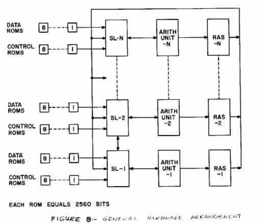
For a unit to accept data from a source the output of the source must be connected to the input of the steering unit for that module. The transfer of data from module to module is a function of the interconnect and the instruction word. Every WA time a new instruction word is transferred from each instruction ROM group to the units in each module. These instruction words define the data path to be selected to each output of each steering unit during the next WO cycle. System operation continues in this manner, WA (instruction fetch), WO (data fetch) until the system executive control resets the instruction ROM's. Data storage ROM's can be treated like the outputs from the other circuits. They are connected to the inputs of the steering units. The total number of ROM's used in each group is a function of the total amount of storage required and the update rate of the system. The number of arithmetic units in a function of the amount of calculation and the update rate of the system. As shown, the hardware is flexible to handle changes in two directions: computational load and update rate. This flexibility is required to handle the various types of systems to be implemented. A general hardware arrangement illustrating the flexibility of the hardware is shown in Figure 8. The final configuration chosen by the user must depend on the total system programming requirements. For the system in Figure 2 the following would be its three instruction word formats.
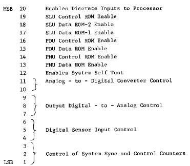
SYSTEM EXECUTIVE CONTROL The system executive control is used to control many parts of the total system. In general, it is used to control the inputs (A/D, discretes, sensor inputs),the outputs (D/A, digital data, discrete), and the processor modules. The system executive control consists of an associated group of ROM's, supplying a 20-bit control word every operation time. Each bit has a preassigned task based upon the hardware configuration. The assignment for each of the bits might be as follows:
System executive control bits 13 through 19 are assigned to control the processor modules. The reason for having such a control is to minimize the storage requirements in the ROM's by disabling their operation when they are not being used.
SOFTWARE COMMENTS The software for this system is closely associated with the hardware arrangement. To program such a system efficiently requires complete knowledge of the hardware. At the present time there is n assembler available to properly handle the multiple instruction set and data path considerations to yield an efficient program. Present programming requires hand coding at the machine code level. This is certainly tedious but it results in a more efficient circuit interconnect and minimum total instruction wards. All of this reflects the number of arithmetic modules and ROM's necessary to handle a particular problem.
ADVANTAGES AND DISADVANTAGES The advantages of such a system are determined by the constraints under which system design was accomplished. The size of the circuit packages were such that the original size constraint was met. The sizes are indicated below:
The flexibility of the hardware to adapt to a great number of problem statements along with its R.O.M. reprogramming capability is certainly a feature desirable in all systems of this kind. The fact that the software and hardware can be used in conjunction with each other helps to reduce the total parts count in the system. When total parts are reduced then power consumption and cost will be reduced. Power consumption for the CPU-Memory discussed in this paper exceeded the original 10 watts. This was due to the large quantity of read-only memory needed to implement the problem statement. With present day technology the cost of such a commercial CPU-Memory system could be less than $2000 in large quantities. This is based on a price of less than $65 per circuit type. The disadvantages of this system is reflected in the software. To hand code the entire program in a machine such as this is a time consuming and tedious effort. To use an assembler or translator to perform the coding would result in a less efficient program and possibly more hardware. To obtain the minimal hardware configuration a person with both hardware and software knowledge of the system is needed. Future designs of this nature need to be worked closer with the software requirements in order to minimize the effort required for programming.
SUMMARY A CPU-Memory system has been presented that satisfied the requirements of a particular application. The "pipelined" approach resulted in a system with enough flexibility to satisfy the present requirement and to adapt to other areas of application. MOS technology provided "state of the art" power dissipations and packaging densities obtainable in no other way. This system proved to be the most effective in meeting the given requirements.
BIBLIOGRAPHY
|
|||||||||||||||||||||||||||||||||||||||||||||||||||||||||||||||
![]()
| Last Updated on 13 September, 2002 | For suggestions please mail the editors |
Footnotes & References